
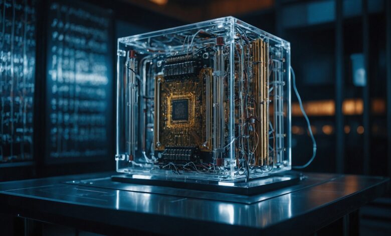
Silicon wafers are essential components in the electronics and semiconductor industries, serving as the foundational material for most integrated circuits (ICs) and microchips. These wafers are sliced from pure silicon crystals and undergo extensive processing to achieve the desired electronic properties. One of the critical parameters of silicon wafers is their resistivity, which determines how well they can conduct electricity and directly affects their performance in electronic devices. Resistivity is a fundamental electrical property that measures the material’s ability to resist the flow of electric current. In the context of silicon wafers, resistivity can significantly influence the overall functionality of semiconductor devices. Higher resistivity materials are typically used in specialized applications like power electronics, while lower resistivity silicon is essential for conventional integrated circuits.
Table of Contents
Introduction of Silicon Wafer Technology
The silicon wafers are the foundation of electronic and semiconductor devices. They play a vital role in the production of microchips and integrated circuits. This section gives an overview of silicon wafers and how they are made. It also explains their importance to electronics.
What Are Silicon Wafers ?
- These wafers, which are primarily made of high-purity silica, are thin slices. These wafers act as the substrate for electronic circuits. These wafers are used in almost all modern electronic devices, such as computers, smartphones and other gadgets.
2.The manufacturing of silicon wafers is an intricate process that requires precision and involves many stages. It begins with the monocrystalline growth of silicon. The Czochralski process is the most commonly used method, which involves growing a single crystal of silicon and then cutting it into thin wafers. These wafers will then be polished and cleaned in order to meet the quality standards required for semiconductor applications.
The Importance Of Silicon In Electronics
- The best material for semiconductors is silicon because it has excellent electrical properties and can form a stable layer of oxide. This makes silicon the ideal material for making transistors, diodes and other important components of integrated circuits.
- Wafers are available in a variety of sizes. Their diameters range from 25mm up to 300mm and beyond. The thickness of wafers varies depending on the application, but must balance mechanical stability with the efficient production and semiconductor devices.
Silicon Wafers: Applications in Modern Technology
- Silicon wafers have many applications. They are used for computing telecommunication automotive electronic and energy solution such as solar cells. Microchips are used in everyday devices like smartphones, laptops and digital cameras.
- Each silicon wafer is subjected to a series of quality checks that ensure its optimal performance. These include electrical tests, surface inspections and thickness measurements. These quality control measures play a crucial role in preventing defects which could compromise the performance and reliability of semiconductor devices.
Emerging trends in Silicon Wafer Technology
- In the evolving world of electronics, the demand for smaller, more efficient, and faster semiconductor devices is increasing. Newer wafer technologies, such as SOI (Silicon on Insulator) and MEMS (Micro-Electro-Mechanical Systems), are being developed to meet these requirements, driving innovation in the industry.
Understanding Resistivity of Silicon Wafers
The resistivity of silicon wafers is an important property that affects their performance in electronic products. This section explores the concept of resistance, how it’s measured, its effects, and its use in semiconductor applications.
What is Resistivity ?
- The resistivity of a material is measured by how much it opposes electrical current flow. It is usually measured in ohm centimeters. Resistivity is used to determine how easily an electrical charge can pass through silicon wafers.
How Resistivity Effects Semiconductor Performance
- Resistivity is a key factor in determining the performance of silicon wafers in various electronic applications. Low-resistivity silicon wafers, for example, are perfect for microprocessors, which require rapid electron movement. High-resistivity silicon wafers, on the other hand, are used in power device applications, where controlling current flow is crucial to avoid overheating.
Factors affecting the resistivity of silicon wafers
- The resistivity of silicon can be affected by several factors, including
- Doping concentration: By adding impurities such as phosphorus or boron, the concentration of charge carriers is changed. This directly impacts resistivity.
- Temperature : As temperature increases, resistivity decreases because there are more carriers available for conduction.
- Crystal Defects : The flow of electrons can be disrupted by defects in the silicon crystal lattice.
Different Types of Silicon Wafers Based On Resistivity
- Wafers with Low Resistivity These wafers are available in resistivity values ranging from 0.001 to 1 O*cm. These wafers are used for high-speed applications, such as processors or memory chips.
- Wafers with Medium Resistivity: These wafers have resistivity values ranging from 1 O*cm to 100 O*cm. They are used in general electronic applications.
- High Resistivity Wafers These wafers are used for applications such as radio frequency devices (RF devices) and power electronics where current flow limitation is important.
Measuring Resistance in Silicon Wafers
- Four-point probe method is a technique that can be used to measure the resistivity of silicon. This method involves placing four electrodes in contact with the surface of the wafer and measuring the voltage drop while the outer electrodes conduct current. This method allows for accurate calculation of resistivity, taking into account factors such as wafer thickness and surface condition.
The Relationship between Doping and Resistivity
- Doping is the addition of impurities to silicon in order to modify its electrical properties. Doping silicon with boron and phosphorus creates either holes that allow electrons to move (p-type) or free electrons. The lower the resistivity the higher the concentration of doping, because more charge carriers can be used for conduction.
The role of resistivity in device fabrication
- The resistivity of silicon wafers determines their suitability for certain semiconductor devices. As an example:
- Wafers with low resistivity can be used to create highly conductive layers for transistors and diodes.
- High resistivity wafers play a crucial role in power electronics. These materials must be able to withstand high voltages while not conducting too much electricity.
Impact on Silicon Wafer Resistance
- Irradiation can further alter the resistivity of wafers. This method introduces defects in the silicon lattice which can increase resistance by disrupting electron flow. In the following sections, we will discuss this in greater detail. We will specifically focus on how irradiation is used to increase and fine-tune the wafer resistance.
Controlling Silicon Wafer Resistance
It is important to control the resistivity in silicon wafers for electronic devices. However, it is not easy to achieve a consistent and precise level of control due various factors. This section examines the challenges in managing silicon wafer resistance and their implications for the semiconductor industries.
Doping Concentration Inconsistent
- The primary way to control resistivity is by doping silicon wafers. Impurity atoms like boron or phosphorus are used. It is difficult to achieve uniform doping across the wafer. Even slight variations in the doping concentrations can cause inconsistencies in resistivity and affect performance in electronic devices which rely on precise electrical properties.
Crystal Defects
- Even the best manufacturing processes may introduce crystal defects. These defects can affect the flow of current and make it difficult to maintain a uniform resistance throughout the wafer. Defects may scatter charge carriers and increase resistivity in some areas, affecting device performance.
Temperature Dependence Resistivity
- Temperature is a major factor in resistivity. Silicon’s resistance decreases as the temperature rises, due to an increased number of charge carriers. Temperature fluctuations in a production environment can cause variations in resistivity between wafers, or even within one wafer. This makes it difficult to maintain consistency electrical properties throughout the manufacturing process.
Surface Oxidation and Contamination
- Air or chemical contamination can cause unwanted surface layers to form during wafer production. These contaminants can affect the electrical properties of a wafer by increasing or decreasing its resistivity. Surface oxidation can occur when silicon reacts to oxygen. This thin layer of insulating material on the wafer complicates the control of resistance during integrated circuit fabrication.
Limitations to Traditional Doping Techniques
- The limitations of traditional doping methods, like diffusion and ion implantation, make it difficult to control resistivity precisely. The movement of atoms in diffusion doping is affected by temperature and time, which can lead to inconsistent results. While ion implantation is more precise, it can cause damage to the crystal lattice of silicon, which affects the wafer’s resistance in unpredictable ways.
Scaling issues in Advanced Semiconductor Devices
- Controlling resistivity is becoming increasingly difficult as semiconductor devices shrink. Even minor variations in resistance can have a significant impact on device performance at smaller scales. Manufacturers are forced to use more advanced techniques in order to achieve uniform resistivity on smaller wafers.
High-Resistivity wafers for Power Electronics
- Power electronics require silicon wafers with high resistivity to withstand high voltages and current leakage. Producing wafers that have extremely high resistance (above 10,000 O*cm), however, is a difficult task. The doping concentrations must be closely controlled. Even small amounts of contamination, or crystal defects, can have a significant impact on resistivity.
Variations in Resistivity of Multilayer Structures
- Multilayer structures are often required in modern semiconductor devices, with each layer having different requirements for resistivity. The manufacturing process becomes more complex when managing resistivity in multiple layers, each of which has its own electrical properties. It is difficult to ensure consistent resistivity across each layer due to the interactions between layers, different doping levels and material properties.
Process Control in Mass Production
- Maintaining tight control of resistivity over thousands of wafers in a mass-production environment is a major challenge. Even minor variations in resistivity can have a significant impact on the performance of large batches of devices. To ensure uniform resistivity, manufacturers must use rigorous process control, such as advanced monitoring and quality assessment.
Conclusion: Future of Irradiation for Enhancing Silicon Wafer Resistance
Irradiation techniques are a great way to improve silicon wafer resistance. These advancements will allow for further refinement of semiconductor manufacturing in the future. They will also enable new applications, pushing the limits of electronic devices. This section examines the potential impact of irradiation on improving silicon wafer resistance and the future of the technology.
Emerging Trends in Irradiation Techniques
- Radiation Sources The Future of Silicon Wafer Irradiation : The innovation in radiation sources will make them more accessible, efficient and environmentally friendly. Compact Neutron Generators, and Advanced Particle Accelerators may become more commonplace in semiconductor fabs. This will allow for a wider use of irradiation to enhance resistivity.
- Improved Control and Precision As irradiation technologies advance, silicon wafers will have greater control over defects. Adaptive Irradiation Systems will allow manufacturers to tune resistivity in real time by modifying energy levels, dose, and exposure patterns.
- Integration of Other Semiconductor Manufacturing Processes
- Seamless integration In the future, irradiation may be seamlessly integrated with existing semiconductor fabrication processes. This integration will lead to more efficient production cycles as irradiation is combined with other steps such as doping, lithography and annealing. Irradiation Chambers may become a standard tool in semiconductor fabs. This will accelerate adoption.
- Hybrid Techniques: There is also potential for hybrid techniques that combine irradiation with other resistivity-modifying methods, such as chemical doping or thermal treatments. These hybrid approaches will allow manufacturers to fine tune resistivity both at the macro- and micro-levels, improving device performance in a wider range of applications.
Expanding applications for high-resistivity silicon
- New Industry Applications As resistivity enhancement technologies improve, new applications will emerge for high-resistivity wafers. Quantum computing 5G/ 6G communication systems Energy storage devices and advanced sensors technology all stand to gain from the advancements in silicon wafer radiation. These new applications are expected to drive the demand for specialized wafers with resistivity-tuned properties.
- Radiation Hardened Electronics With the growing need for electronics to withstand harsh environments such as nuclear reactors or space, irradiation enhanced resistivity is becoming more important. The next generation radiation hardened electronics will require silicon wafers with stable electrical properties and radiation resistance.
- Environmental and Safety Considerations
- Sustainable Practices As irradiation becomes more common, the industry will concentrate on minimizing the environmental impact. Sustainable Irradiation Technologies will be key in reducing the carbon foot print of semiconductor manufacturing.
- Radiation Safety While irradiation has many benefits, there are also safety concerns because of the high-energy particles used and radioactive sources. Improved safety protocols and Shielding techniques as well as Automated Handling Systems ensures that the risks of irradiation are kept low. This allows for safer and more responsible industrial use.
Scalability Challenges and Opportunities
- Overcoming the Scalability Challenges As demand for silicon wafers with high resistance grows, scaling will become a major concern. Scaling up electron and neutron irradiation, for instance, can be expensive and time-consuming. high throughput irradiation system, and batch process innovations could help address these challenges. Irradiation would then become a cost effective solution for mass production.
- Customization Opportunities One of the main advantages of irradiation lies in its ability to produce custom resistivity profile tailored for specific applications. Manufacturers will be able to create highly customized wafers that are optimized for consumer electronics, medical devices and aerospace technology.
Future Research Directions
- Advanced Simulation Tool: Scientists and engineers will be able to predict better the effects of irradiation of silicon wafers with the development of advanced Simulation Models. These tools will allow for more precise experimentation, and optimization. This will reduce the need for trial-and error approaches in manufacturing.
- Exploring New Materials While silicon is still the most common semiconductor material, future research will likely explore the effects of irradiation on other materials such as galium nitride, silica carbide and emerging materials such as graphene. Understanding how irradiation enhances the properties of these material will lead to new opportunities for improving device performance.
- Irradiation of Next-Generation Semiconductor Devices
- Smaller Devices, Faster and More Efficient The future of semiconductor devices will be smaller designs, faster and more energy efficient. Manufacturers will be able reduce power consumption by improving thermal management through the use of irradiation. This will lead to longer battery lives and better performance for devices such as smartphones and electric vehicles.
- The Future of Moore’s Law As Moore’s Law nears its physical limit, irradiation could offer a solution to prolong the life of silicon-based technology. Irradiation can allow further miniaturization by enhancing resistivity, controlling defect formation and reducing the amount of material used.
Market Growth and Economic Impact
- Growth of the Semiconductor Industry With the increasing demand for advanced electronic and the proliferation technologies such as AI, IoT and autonomous vehicles the semiconductor industry will experience significant growth. The industry for high-resistivity wafers is set to expand as irradiation technologies become more cost-effective and accessible.
- Increased competition As irradiation becomes more common, the competition between semiconductor manufacturers will grow. The global market will be dominated by those who can use irradiation more effectively and efficiently to increase wafer resistance.